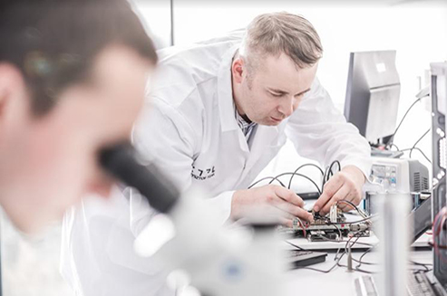
XTPL is shaking hands with Wise Device Inc., the Canada-based global leader of industrial microscopy automation development. The company is interested in using the XTPL technology in the process of removing display matrix defects that occur at the production stage. The collaboration plan has been confirmed by a letter of intent.
Wise Device Inc. was established in 2005. It develops and provides innovative microscopy automation systems for the semiconductor industry, including the key players from the sector of display technology. At present, its customers include businesses from Korea, Japan, Taiwan, China, the U.S. and Europe.
– It often happens that during the production process of liquid-crystal displays some defects crop up in the conductive films of the matrix, e.g. in the form of broken electronic links. The existing technology for eliminating such defects is based on LCVD (Laser Chemical Vapour Deposition). Hoverer, it is extremely complex and uses toxic and hazardous gases. The Canadian company has analysed the capabilities and results of the XTPL technology and concluded that our method for printing ultra-thin conductive lines can prove much more effective in doing away with such limitations of the modern-day standard on the market of technologies used for repairing local defects in metallic structures. Commencing the collaboration with Wise Device, we are actively entering the rapidly developing niche in the global display market. As a result, we will soon start working with the top global producers in the sector of electronics, says Dr Filip Granek, CEO at XTPL.
The common goal of XTPL and Wise Device Inc. is to develop specialized technologies and devices to be used in the production of LCDs. The companies will focus on developing a method for removing local defects in metallic links in the TFT (Thin-Film Transistor) matrices, i.e. the key elements of LCDs.
– The unique feature of XTPL’s technology is the possibility to print very thin (down to the submicron level) electrically conductive structures. Such a technology can vitally improve the LCD production performance, since it is capable of eliminating defects that occur during the production process itself. The complementary competences of both teams (Wise Device Inc. and XTPL) will allow to develop and provide a unique printing system for this segment of the market, wrote Dr. Adam Weiss, CEO at Wise Device, in the letter of intent.
Based on the capabilities of the XTPL technology, one may predict that XTPL will reach a double-digit share in this segment within the next two years.
It is only one of the numerous possible applications of the XTPL technology. Ultra-thin electrically conductive lines can be used in the production of solar cells and displays as well as in printed electronics, microelectronics, biosensors, nanophotonics, microphotonics, smart windows and anti-counterfeit solutions. At the printed electronics trade fair in Berlin, international enterprises operating in the above industries showed interest in collaborating with XTPL.
Wise Device Inc. designs, engineers and manufactures innovative microscopy automation solutions, including OEM components as well as complete optomechanical and optoelectronic sub-systems. WDI’s technology helps individuals and companies in a wide variety of industries including Life Science, Biomedical Imaging, Machine Vision and Electronics/Semiconductor Manufacturing. Its solutions are currently used by well know organizations such as Intel, Corning, Apple, Samsung and LG.
Source: XTPL
Photo © XTPL


